Perovskites: Versatile Semiconductors
Halide perovskites are rock-star semiconducting materials that have emerged in the past decade because of their extraordinary physical properties, and they have outperformed many rival materials from other classes of compounds in a wide variety of optoelectronic applications. The perovskites are three-dimensional (3D) structures of metal halide networks with the general formula AMX3. Their 3D structure creates a favorable environment and electronic band structure facilitating charge transport.
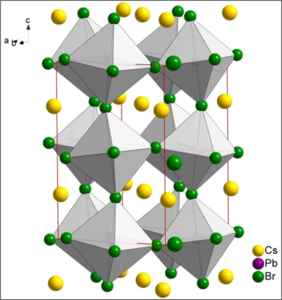
One well-studied perovskite, CsPbBr3 (CLB), features a large bandgap of 2.3 eV which ensures low dark currents and robust performance well above room temperature. CLB has a pseudo-cubic perovskite structure (Figure 1).
Actinia is developing technology, first invented at Northwestern University, based on all-inorganic CLB materials which manifest competitive performance in -ray and X-ray detection. Compared to organic-inorganic hybrid perovskites, the all-inorganic CLB perovskite features great advantages in chemical and device stability, due to lack of organic molecules, while also exhibiting top-of-the-line performance that rivals the best room-temperature semiconductors. Unlike such materials, however, detector-quality CLB is inexpensive to synthesize, uses readily available starting materials, and tolerates crystal defects well.
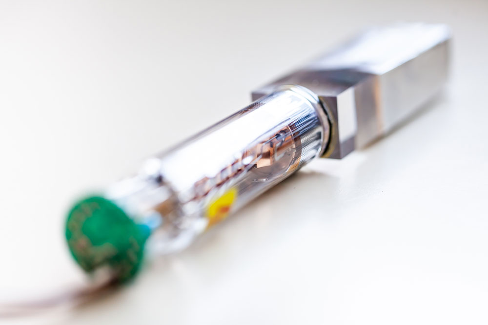
Actinia has developed proprietary growth methods for high-quality crystal growth of CLB. Growing crystals of CLB using Actinia’s techniques has the advantage of producing size-controllable high-purity single crystals and provides a feasible path to mass production for commercial X-ray detection applications. Actinia’s proprietary crystal growing technology produces high-performing large CLB crystals, Figure 2. Actinia’s CLB devices exhibit high energy discrimination ability and high X-ray sensitivity under a variety of X-ray sources with a continuum energy spectrum.

Gamma Ray Detection
Nuclear detection for the purposes of homeland security and industrial safety requires high sensitivity and resolution, to allow the detection of distant, shielded, or weak nuclear radiation sources. To be effective, it also requires low-cost detection to allow broad-based implementation. The most important type of radiation emitted from fissile materials is γ-rays of a wide variety of energies. The ideal detection material would convert the energy of incident radiation quanta into a distinct optical or electrical signal that accurately transmits information about the incident radiation.

The two primary categories of γ-ray and X-ray detection media are scintillators and semiconductors. For both types, the radiation detection process begins with the absorption of photons and the creation of primary energetic charged particles. Semiconductors are generally superior to scintillators because they offer significantly higher energy and spatial resolution in detection. In many applications, such as non-destructive inspection by X-ray systems (important in detecting contraband, such as illicit drugs, radiological materials, and special nuclear materials), intense, high-energy X-ray sources with energies up to tens of MeV are needed, which is challenging for scintillator-based detectors.

When γ-radiation enters a semiconductor, a complex cascade of energy transfer interactions occurs. This results in the production of a large number of electrons and holes which end up in the bottom of the conduction band and top of the valence band respectively. The physical region in which the complex cascade of energy transfer interactions occurs in the solid material is referred to as a ‘track’. The mobile charge signal in semiconductor detectors is then collected directly using high electric fields to sweep charge to surface electrodes, placing a premium on the material’s charge transport properties. A successful semiconductor radiation detector material should have good stopping power, must be obtainable as large high-quality crystals at low cost, have acceptable carrier mobilities and lifetimes, and operates at ambient temperatures, but current materials have various limitations that motivate the development of new materials.
The currently available g-ray detector semiconductor materials have been known for over forty years and still face many challenges, including high cost and low yield. CdZnTe (CZT) is dominant as the current room temperature radiation detection material, however, its applications are severely restricted because of high cost and unsolved issues in crystal growth. With great advances in chemistry and physics, the understanding of semiconductor materials and their physiochemical properties has considerably increased over the last two decades. We can now predict, design and screen novel semiconducting compounds that meet the selection criteria for high detection performance. We have accelerated novel nuclear detector material discovery and created next-generation radiation detection at room temperature. Recently, we showed that CsPbBr3 can compete with the resolution of CZT at a much lower cost. New materials and their insertions into advanced technologies are essential for a variety of applications such as medical imaging diagnostics, industrial imaging, and quality control, and in detection of smuggled nuclear materials and weapons of mass destruction.
X-Ray Detection
The great demand of X-ray imaging towards lower dose and higher resolution has required rapid evolution of X-ray detection systems over the past decades. In such systems, a fluence of X-ray photons is applied, possessing a continuous spectrum of energies generated by Bremsstrahlung interactions. Two general signalizing modes, in terms of energy-integrating and photon-counting, are utilized for semiconductor X-ray detectors operated at room temperature. Energy-integrating mode integrates the total energies deposited in the detectors over a certain time period with no regard to quantifying the number and energy of incident photons, whereas the photon-counting mode is capable of discriminating the energies of individual X-ray photons. Due to the significant enhancement of the imaging contrast and reduction in the radiation dose, photon counting X-ray detectors are aimed to revolutionize X-ray imaging in the future. New materials, such as Actinia’s, CsPbBr3, are poised to facilitate this revolution.

Key Publications
- “Crystal Growth of the Perovskite Semiconductor CsPbBr3: A New Material for High-Energy Radiation Detection”, Stoumpos, C. C.; Malliakas, C. D.; Peters, J. A.; Liu, Z. F.; Sebastian, M.; Im, J.; Chasapis, T. C.; Wibowo, A. C.; Chung, D. Y.; Freeman, A. J.; Wessels, B. W.; Kanatzidis, M. G., Cryst. Growth Des. 2013, 13 (7), 2722-2727.
- “High Spectral resolution of gamma-rays at room temperature by perovskite CsPbBr3 single crystals”, He, Y. H.; Matei, L.; Jung, H. J.; McCall, K. M.; Chen, M.; Stoumpos, C. C.; Liu, Z. F.; Peters, J. A.; Chung, D. Y.; Wessels, B. W.; Wasielewski, M. R.; Dravid, V. P.; Burger, A.; Kanatzidis, M. G., Nature Communications 2018, 9, 8.1609.
- “Perovskite CsPbBr3 single crystal detector for alpha-particle spectroscopy,” He, Y. H.; Liu, Z. F.; McCall, K. M.; Lin, W. W.; Chung, D. Y.; Wessels, B. W.; Kanatzidis, M. G., Nuclear Instruments & Methods in Physics Research Section a-Accelerators Spectrometers Detectors and Associated Equipment 2019, 922, 217-221.
- “CsPbBr3 perovskite detectors with 1.4% energy resolution for high-energy gamma-rays”, He, Y. H.; Petryk, M.; Liu, Z. F.; Chica, D. G.; Hadar, I.; Leak, C.; Ke, W. J.; Spanopoulos, I.; Lin, W. W.; Chung, D. Y.; Wessels, B. W.; He, Z.; Kanatzidis, M. G., Nature Photonics 2021 15, 36–42


